Designing an electrical circuit for connecting to Ethernet 10BASE-T
In this post I discuss an electrical circuit design for connecting a microcontroller to an Ethernet 10BASE-T network using a differential transceiver. I then describe how to perform a rudimentary validation of the electrical circuit using a few lines of code and an oscilloscope. This post is part of a series of posts relating to Niccle, my Ethernet 10BASE-T bit banging project.
In my previous post I provided a high-level overview of Ethernet 10BASE-T. In the coming sections I'll give a brief summary of the electrical components that make up an Ethernet circuit (focusing on the 10BASE-T version), I'll show the concrete electrical circuit that I chose to use, and I'll discuss the choices that led me to that design. This was as much an exercise for me in designing a circuit for my specific purposes, as it was an exercise in trying to understand why everybody else's circuits are designed the way they are. Hopefully my write-up can be of use to others in the future.
I'll then show how we can write a minimal amount of code to show that we can use the circuit to actually connect our microcontroller to another device, making that device think that a link has been established. Lastly, I'll also perform a few basic signal integrity checks over the circuit to gain some confidence that the circuit will actually allow us to transmit and receive data in practice. While none of these checks will conclusively prove that circuit is fully functional, they're useful as an initial validation before we dive deeper into the actual transmission and reception of data.
Table of Contents
The components of an Ethernet circuit
With Ethernet 10BASE-T operating in full-duplex mode, a connection between two devices forms two electrical circuits, one across across each of the two wire pairs used in the Ethernet cable. Each circuit connects one device's transmitter with the other device's receiver and vice versa. Thus, each Ethernet connection consists of two simplex links, each allowing data to be sent in only one direction. Let's take a high-level look at the components each these simplex links consist of.

An abstract representation of the circuit formed by a simplex Ethernet link across a single wire pair. Each Ethernet 10BASE-T connection consists of two such simplex links, in opposite directions.
On the transmission side of the link we have:
- A transmitter component that takes a digital output signal
DO(high or low) and emits an equivalent differential signalTX(e.g. +2.5 V or -2.5 V) over a pair of output wires. - A balun component, reflecting the fact that the circuit formed by the cable's twisted pairs is a balanced line, while the transmitter's outputs may be unbalanced.
- A component that performs galvanic isolation, to ensure that there is no conductive path between the two devices connected to each end of the cable.
- A connector that allows a cable to be connected to the device. Usually this is an 8P8C connector (commonly called an "RJ-45" or "Ethernet connector").
While on the receiving side we have:
- Similar components for the cable connector, galvanic isolation, and balun.
- A load across the wires in the wire pair, which ensures that the receiving side's impedance is matched to the characteristic impedance of the transmission line itself.
- A receiver component that takes the differential input signal
RXand emits an equivalent digital signalDI(high or low).
And of course between the transmission side and the receiving side we have the Ethernet cable connecting the two. Twisted pair cables used for Ethernet must have a characteristic impedance of 100 Ω.1 The cable forms a transmission line, and hence transmission line effects must be taken into account (e.g. by impedance matching the circuits connecting to the line), since cables can be up to 100 m in length, much longer than the ~30 m wavelength of a 10 MHz signal.
It's worth noting that in a real circuit a single component may take care of multiple abstract components in the above schematic. For example, Ethernet circuits generally use a transformer between the connector and the TX/RX circuits, acting as both the balun and the galvanic isolator. In some cases the connector and transformer are even packaged into a single component, taking care of all three roles at once. The connector is said to have "integrated magnetics" in that case.
Now let's take a look at how we can realize this abstract circuit in practice.
My Ethernet circuit
For my project's circuit I used a dedicated differential transceiver IC to drive and read the differential signals. I also chose to use an Ethernet connector with integrated magnetics since it meant I could simplify the circuit a bit further. The following circuit is what I eventually landed on:

An Ethernet circuit using an ISL3177EIBZ differential transceiver and an 8P8C connector with integrated magnetics. The DI & RO pins of the ISL3177E correspond respectively to the DO & DI pins of the abstract schematic above, and can be connected directly to the microcontroller's GPIO pins.
The components were chosen as follows:
U1: an ISL3177E differential transceiver. I chose this chip mainly because a few other projects referenced or used it already, and I didn't want to spend too much time looking for alternatives. It supports the 10 MHz max frequency used by Ethernet 10BASE-T, and has a convenient 8SOIC form factor. However, in hindsight the ISL3176E variant might've been a better choice, as it supports an output-enable function, whereas the ISL3177E does not (more on this below).- Note that the ISL3177E chip uses the name
DIfor the driver input pin that specifies which signal the transmitter should emit. Hence, itsDIpin actually corresponds to theDOlabel in the abstract circuit diagram in the previous section. - Its
ROpin is the receiver output which reflects the received signal. Hence, it maps to theDIlabel in the abstract circuit above. - The abstract circuit diagram uses the same terminology as the IEEE 802.3 standard document, hence the discrepancy.
- Note that the ISL3177E chip uses the name
C1: a bypass capacitor to ensure a steady power supply to the ISL3177E IC. The value of 100n is based on the ISL3177E datasheet's example circuits.C2andC3: AC-coupling capacitors on the outgoing transmission line. The value of 10 nF was chosen empirically. These are discussed more in the section below).C4andC5: these may help reduce the common-mode noise in the signal. I didn't observe any significant difference in the signal quality with or without these, but it's pretty standard practice to terminate the center taps of the isolation transformers this way.R1: a load-end termination resistor. The ISL3177E's receiver inputs have a high impedance of at least 96 kΩ, so we need this resistor to ensure the line is impedance-matched to the transmission line's differential characteristic impedance of 100 Ω, as required by the IEEE 802.3 spec.2 Without it we'd get significant signal reflections on the line.R2andR3: source-end termination resistors on the transmission pins, which I added mainly to attenuate the signal voltages to ensure they fall below the 3.1 V threshold specified by the IEEE 802.3 standard, but which also help impedance-match the source-end of the transmission line. These are discussed more in the section below.
The following sections describe a few of these choices in more detail.
AC-coupling capacitors C2 and C3
The AC-coupling capacitors ensure that output pins Y and Z of the ISL3177E
chip aren't shorted through the transformer they're connected to, i.e. no DC
current can flow between them. This is important because the ISL3177E chip is
always-on, which means that there's always a non-zero voltage between Y and
Z. This means that if they're shorted a (substantial) DC current will flow
between them. This can be up to 250 mA according the datasheet, although I
measured it closer to 40 ma in my circuit when I removed the AC-coupling
capacitors.
This is the reason why a chip like ISL3176E could've been a better fit, as its
output-enable function would allow the Y and Z pins to be disabled when the
receiver is idle, in which case they serve as high impedance inputs between
which no current would flow. This could possibly avoid the need for the AC
coupling capacitors completely. It would, however, require the use of an
additional GPIO pin to drive the output-enable signal.
When I used a smaller value of 4.7 nF it caused more signal attenuation, especially for low-frequency parts of a transmission, like the 250 ns long TP_IDL pulse. On the other hand, higher values like 47 nF caused transmitted signals to take longer to become centered around a 0 V level. Hence, 10 nF seemed like a good compromise. Note that these effects are discussed further in a later section.
Note that it is fine to AC-couple our transmission circuit this way, because Ethernet 10BASE-T uses the Manchester encoding, which ensures that the resulting signal is DC-balanced.3
Source-end termination resistors R2 and R3
In addition to the AC coupling capacitors, I also used source-end series termination resistors of 50 Ω (49.9 Ω to be precise) on each of the TX pins. These attenuate the transceiver's output voltage a bit, ensuring that peak signal voltage (e.g. during a link test pulse) remains below the specified 3.1 V. Without these resistors, the observed voltage was around 3.4 V, while this is reduced to about 2 V when using these resistors.
Since the termination resistors' values match the transmission line's differential characteristic impedance they also have a secondary beneficial effect of impedance matching the source-end of the transmission line. This helps attenuate any signal reflections from the returning from transmission line. In general we don't expect there to be a significant level of signal reflections to begin with, since the load-end of the transmission line is supposed to be properly terminated with a 100 Ω resistor that matches the differential characteristic impedance of the transmission line, but the source-end resistors will further attenuate any reflections that do occur, and technically speaking source-end impedance matching is also prescribed by the IEEE 802.3 standard anyway.4
Inverting the incoming RD+/RD- signals to the receiver
Lastly, you may have spotted that pins A and B are the non-inverted &
inverted differential receiver inputs on the ISL3177E chip, respectively, yet I
connected A to RD- and B to RD+ (rather than the other way around). This
arrangement will make a positive signal on the line look negative to the
receiver, and vice versa.
The reason for this choice is that the ISL3177E chip considers any signal above -50 mV to be "high", and only signals below -200 mV to be low (the datasheet refers to this as a "Full Fail-Safe" function that ensures a high signal is produced when the inputs are shorted or disconnected). This functionality is useful when the transceivers are used for the main intended purpose: participating in the RS-485 or RS-422 protocols.
That's problematic for their use with Ethernet though, especially if we want to be able to detect incoming link test pulses (LTPs). These pulses allow us to distinguish a disconnected line from a connected one (see the Ethernet overview in my previous post for more info). LTPs are short pulses of a positive signal between 0.585 V and 3.1 V, which are sent during periods when the line is otherwise idle (i.e. when it is at 0 V signal level). If we were to consider any signal above -50 mV to be high, then we wouldn't be able to distinguish between an idle line and an incoming LTP since the line would simply look consistently high!
By inverting the receiver inputs, an idle line will result in a high digital output signal from the transceiver when the line is idle, but a link test pulse will result in a low digital output signal, allowing us to distinguish an disconnected line from a connected one. You can see this in action the section below. It does mean that all incoming data signals will be inverted as well, but that can be reverted easily enough in software.
Why not connect directly to GPIO instead, without a differential transceiver?
My use of a differential transceiver is different from some of the other projects I referenced in the prior art section of my previous post. The holysnippet/pico_eth project connected the GPIO pins directly to the isolation transformer, for example, resulting in a more minimal circuit consisting largely of passive components.
I chose to use a dedicated transceiver because it meant that I would only need to drive a single GPIO pin for outgoing transmissions (which could make bit banging the high frequency signals a bit easier), whereas connecting GPIOs directly to the transformer requires a pair of pins driven to opposite values. It also meant I didn't have to worry about protecting my microcontroller's pins from high voltages, since the active transceiver takes care of those concerns. Lastly, I was also curious to see how clean of a signal I could achieve with a dedicated transceiver, and consequently how low of a packet loss rate I could achieve.
Validating the circuit
Now that I've shared the circuit I landed on, I'll discuss how we can validate its function. Broadly speaking I'll discuss three validation steps:
- Confirming (with an oscilloscope) that we can observe incoming link test pulses when the circuit is actually connected to another device.
- Confirming that the output signals have appropriate voltage levels and shapes, by connecting our circuit to a dummy passive load, transmitting a few signal patterns, and observing them with an oscilloscope.
- Confirming that we can send outgoing link test pulses, and that this makes the other device think that a connection has been established.
Note that, as discussed in my
Niccle project introduction post, I'm
using an ESP32-C6 microcontroller with a 160 MHz CPU clock, and I'm using the
esp-rs/esp-hal framework. It's also worth
noting that all of the steps in the following sections were performed with a
breadboarded version of the circuit, since I haven't produced a PCB yet. In this
breadboarded version of the circuit I used standard through-hole capacitors and
resistors, and for the source-terminating resistors R2 and R3 I used values
of 47 Ω rather than 50 Ω. Otherwise the breadboarded circuit was equivalent
to the schematic shown above.
Validating incoming link test pulse waveforms
Let's start by looking at the RX circuit, specifically whether we can detect incoming link test pulses, and if so, whether their signal levels are as expected.
We'll connect the our receiver circuit to an Ethernet cable that is connected to
a computer, and we'll attach an oscilloscope to both the incoming RX wire pair
as well as to the ISL3177E transceiver's RO pin to inspect incoming signals.
We won't connect the transceiver's output pins to the TX wire pair yet.
As shown below, we can see incoming test pulses by setting the oscilloscope to
trigger on a falling edge on the transceiver's RO pin. We trigger on a falling
edge because as discussed above the transceiver will
invert the incoming signal, turning incoming positive differential signals into
negative digital signals.
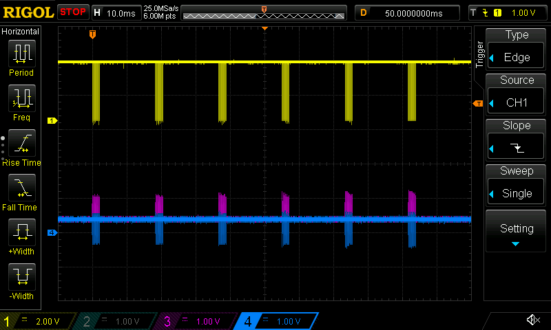
An oscilloscope screenshot with two traces at the bottom representing the incoming differential signal, and the trace at the top representing the corresponding inverted digital signal output by the differential receiver. The screenshot shows bursts of incoming fast link pulses (FLP), each burst 16 ms apart.
The oscilloscope screenshot actually shows that we're receiving fast link pulse (FLP) bursts, which are short bursts of multiple link test pulses, each burst 16 ms apart, rather than just a single pulse every 16 ms. We're seeing these because my computer's Ethernet port supports faster versions of Ethernet than just 10BASE-T, and has the Ethernet autonegotiation feature enabled by default. The autonegotiation feature and FLPs were introduced in later IEEE 802.3 standards, but are backward compatible with devices that only supports 10BASE-T.5
Let's take a closer look at a single one of these FLP bursts.
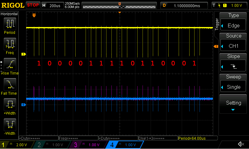
An oscilloscope trace showing a zoomed in view of a single incoming FLP burst. Note the x-axis uses 200 μs time steps, compared to the 10 ms time steps in the earlier image. The pulses in the burst are either 62.5 μs or 125 μs apart.
Each FLP consists of 17 link test pulses 125 μs apart, and encodes 16 bits of
data using 16 optional pulses between each of those 17 pulses. Optional pulses
that are present represent a logical 1 and absent ones represent a logical 0.
The particular FLP above therefore encodes the value 10000111 10110001, which
indicates that the device supports both 10BASE-T and 100BASE-TX, in both half
and full duplex modes, as well as (asymmetric) pause frames (see the
Wikipedia page on autonegotiation
for details on decoding this data).
If we force the Ethernet interface to not use the autonegotiation feature (e.g.
using sudo ethtool -s {the_interface} autoneg off speed 10 duplex full on
Linux), then we can see that only individual link test pulses, rather than
bursts of fast link pulses, are sent every 16 ms.
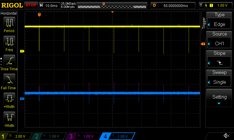
An oscilloscope screenshot showing individual incoming link test pulses about 16 ms apart.
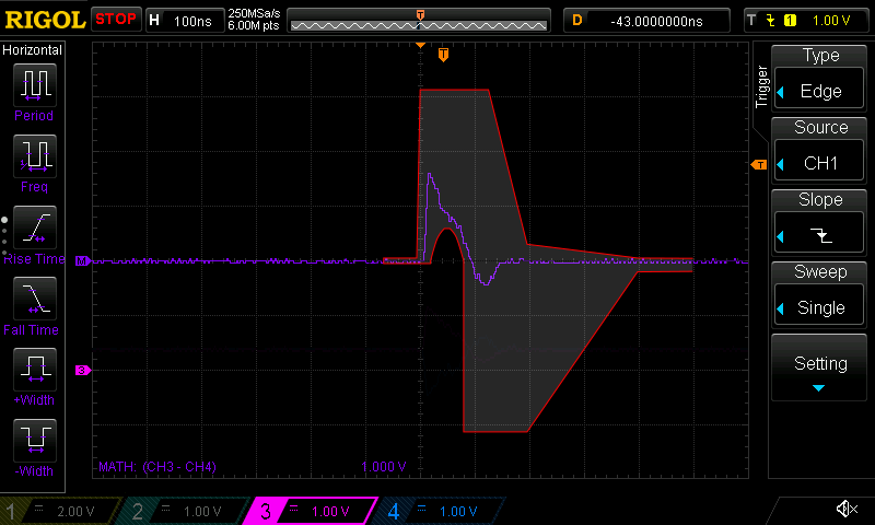
Let's take a closer look at a single link test pulse. In the screenshot below I've used my oscilloscope's math function to calculate the delta between the two incoming signal pairs, thereby calculating the actual logical differential signal value.6

An oscilloscope screenshot showing an individual incoming link test pulse trace, calculated by taking the delta of the incoming signal pairs using the math function of the oscilloscope.
We can see that the incoming differential signal is 0 V until the pulse starts, that the pulse reaches a peak differential voltage of about 1.7 V and that it lasts about 80 ns before briefly going negative and then settling at 0 V again.
We can also see that the ISL3177E transceiver correctly picks up the pulse (albeit with a delay of about 135 ns), with an initial high output level, followed by a low 0 V output for 110 ns long corresponding to the incoming pulse, followed by a high output level again. Note that the transceiver's digital output is the inverse of the input, as discussed above.
So far our receiving circuit looks to be working well enough to detect incoming link test pulses!
The link test pulse waveform template
The IEEE 802.3 standard actually defines a waveform template that link test pulses have to adhere to.7 It is this template that specifies that a link test pulse must have at least 60 ns of a positive signal with a voltage above 0.585 V but less than 3.1 V. An adapted version of that template is shown below.

The waveform template that link test pulses must fit
within.
(Adapted from Figure 14–13 of the IEEE 802.3 standard document.)
If we overlay this template on top of an incoming link test pulse trace, we can see that the incoming pulse fits within the template, as required by the spec.
An oscilloscope screenshot showing another incoming link test pulse, but now with the waveform template overlaid. The pulse fits neatly within the template.
We'll use this waveform template in the next section as well, to validate that our own TX circuit generates waveforms that fit the spec as well.
Validating outgoing link test pulse waveforms
Now that we've established that we can at the very least receive incoming link test pulses correctly, let's take a look at whether we can transmit outgoing pulses over the TX circuit as well. Before we go as far as connecting the TX circuit to a real device, we'll first take a look at the output waveforms that the TX circuit generates, to validate that they fall within the template we just discussed.
Generating a link test pulse using GPIO
It's easy enough to write some code to emit a link test pulse over our TX circuit every 16 ms.
unsafe
A function that generates a link test pulse of 62.5 ns long every 16 ms via GPIO. Full source on Github.
The code simply outputs a signal via GPIO, which the ISL3177E transceiver will then turn into a differential signal that gets transmitted across the cable.
Note that this code uses the dedicated IO mechanism to perform high-speed GPIO (see my previous post on the GPIO speed of ESP32-C6 microcontrollers for more info). Since our CPU frequency is 160 MHz, each instruction takes 6.25 ns to execute.
The generated link test pulse waveform
Now let's take a look at the link test pulse waveform that this code generates over our TX circuit. To do so, I'll connect the circuit to an Ethernet cable, and then I'll terminate the other end of the cable with another Ethernet connector with integrated magnetics, which in turn has a 100 Ω termination resistor attached to our TX pins but which is otherwise not connected to anything else. I.e. I won't actually connect our circuit to a real device yet. I'll use a 50 ft length of CAT-5E cable, because that's the longest cable I have lying around.
This setup simulates a real situation where the cable is connected to a real device, but allows us to inspect the signal as it would look to the receiving device, rather than just inspecting what the signal looks like on the source-side of the cable. For example, this setup will allow us to take the attenuation and the delay of the signal across the cable into account, at least to some extent.
With this setup, we can observe the following waveforms over the Ethernet cable.
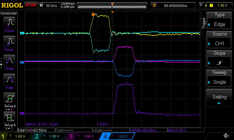
An oscilloscope screenshot showing an individual outgoing link test pulse. The top two traces show the outgoing signal pairs at the start of the cable (between the AC-coupling capacitors and the connector's transformer), the middle two traces show the outgoing signal pairs at the end of the cable across the 100 Ω load, and the bottom trace shows the delta between those two signal pairs (i.e. the actual differential signal across the load). Not shown in this screenshot is the GPIO-to-transceiver signal, since I only have four inputs on my oscilloscope.
Instead of looking only at the waveforms at the start and end of the cable, we can also look at the digital GPIO-to-transceiver signal, as in the screenshot below.
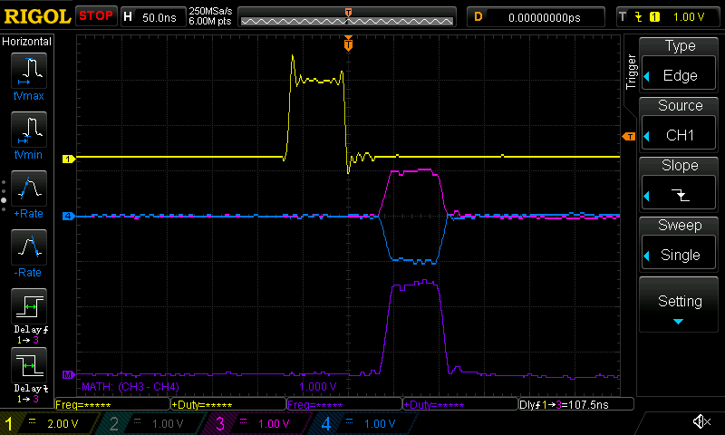
An oscilloscope screenshot showing an individual outgoing link test pulse, similar to the screenshot above, but showing the GPIO-to-transceiver signal this time. The top trace shows the GPIO-to-transceiver signal, the middle two traces show the outgoing signal pairs at the end of the cable across the 100 Ω load, and the bottom trace shows the delta between those two signal pairs (i.e. the actual differential signal across the load).
In general, the bottom MATH trace is what we ultimately care most about, as it corresponds to the logical signal we're trying to transmit. For the most part I'll stick to showing these four sets of traces in the sections below, as they convey nicely how the signal travels across the our circuit, from the initial GPIO output (the top trace), to the differential signal pair on the cable (the middle traces), to the logical signal that pair of values represents.
As you can see, we get a nice squarish, symmetrical waveform on the TX wire pair on both sides of the cable, with a peak differential voltage of around 2 V measured across the termination resistor at the end of the cable. As I noted earlier, this is due to our use of source-end termination resistors. Without those source-end termination resistors, I saw a much higher peak voltage of around 3.4 V, which is more than 3.1 V maximum voltage prescribed by the IEEE 802.3 standard.
Indeed, if we overlay the link test pulse waveform template on top of one of our generated pulses, we can see that it fits nicely within the bounds of the template.
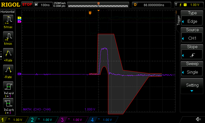
An oscilloscope screenshot showing a close-up view of an outgoing link test pulse, with the waveform template overlaid. The outgoing pulse fits neatly within the template.
The signal delays introduced by the CAT-5E cable and the digital transceiver
Before moving on, I think it's interesting to point out that the above screenshots also show the signal delay that is incurred by transmitting the signal across the 50 ft long Ethernet cable, and through the ISL3177E transceiver.
In the first screenshot, the signal arrives at the end of the cable about 83.5 ns after it appears at the start of the cable. This matches almost exactly what we expect, since the speed of light is about 0.3 m/ns, the velocity factor of CAT-5e twisted pair cabling is about 64%, and hence an electrical signal will travel over the cable at approximately 0.19 m/ns. This results in a calculated total travel time of about 79 ns for a 50 ft long cable. I thought it was quite interesting to be able to see the speed of signal propagation on the wire so clearly.
In the second screenshot we see that that the delay between the GPIO-to-transceiver signal and the signal at the end of the cable is 107.5 ns. Hence, we can conclude that the transceiver introduces its own delay of about 24 ns here (107.5 ns minus 83.5 ns), which is right around the 27 ns typical value listed for the "Driver Differential Output Delay" spec in the ISL3177E datasheet.
Using link test pulses to establish a connection
We've now confirmed that the link test pulse waveform we're generating looks good. Our code is already generating this link test pulse periodically every 16 ms, which should be sufficient to make a connected device think that a link has been established when we connect it to our circuit.
Indeed, when connecting the cable to my Linux computer using the default network
connection settings (i.e. re-enabling the autonegotiation that I disabled
earlier), we see the following ethtool output:
$ sudo ethtool enp108s0
Settings for enp108s0:
Supported link modes: 10baseT/Half 10baseT/Full
100baseT/Half 100baseT/Full
1000baseT/Full
Supports auto-negotiation: Yes
Advertised link modes: 10baseT/Half 10baseT/Full
100baseT/Half 100baseT/Full
1000baseT/Full
Advertised auto-negotiation: Yes
Speed: 10 Mb/s
Duplex: Half
Auto-negotiation: on
MDI-X: on (auto)
Link detected: yes
Success! Note how it says Link detected: yes at the bottom, indicating that my
computer thinks a device has been connected to its Ethernet port.
Also note how it says Speed: 10 Mb/s, Duplex: Half, and
Auto-negotiation: on. This indicates that the interface's auto-negotiation
implementation determined that our circuit only supports Ethernet 10BASE-T in
half-duplex mode. This makes sense, because we're not emitting any FLP bursts at
all, in which case the the autonegotiation protocol assumes the lowest common
denominator capability.
Validating outgoing data transmission waveforms
As a last validation step before moving on to trying to use the circuit for actual data transmissions in my next post, I'll a look at how the circuit behaves when we generate waveforms that mimic what real data transmissions will look like.
To do so, I'll write some code to generate three categories of waveforms in sequence: a 5 MHz waveform that corresponds to the preamble in a real transmission, followed by alternating 10 MHz and 5 MHz waveforms corresponding to an Ethernet packet's varying encoded 0 and 1 bits, followed by a positive pulse of 250 ns corresponding to the TP_IDL signal that will trail each data transmission. As long as the circuit transfers each of these parts of the signal adequately (without too much attenuation, noise, or signal reflections), then we can be fairly confident that it will work well in real use as well.
Generating a simulated data packet using GPIO
The function below generates the first part, the 5 MHz waveform. I won't include the code that generates the other parts of the test waveform here since it's a bit long and repetitive, but you can click the link below if you want to see them. Note that I'm again using the dedicated IO mechanism to perform high-speed and precisely-timed GPIO.
unsafe
The first part of a function that generates a waveform that simulates a real packet transmission. The code shown produces 5 MHz waveform just like we would see with a real packet's preamble. Full source on Github.
The generated simulated data packet waveform
Now let's take a look at what the generated waveform actually looks like on our circuit. I'll again connect our circuit to an Ethernet cable that is terminated with a 100 Ω termination resistor, so we can inspect the signal as it would look to a receiver at the end of the cable.
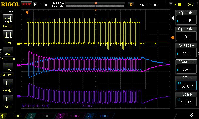
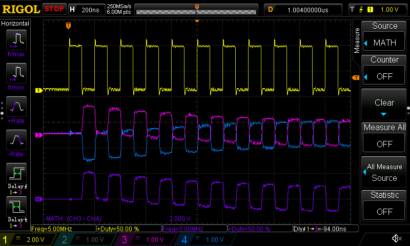
An oscilloscope screenshot showing an outgoing signal for a simulated data packet. The top trace shows the GPIO-to-transceiver signal, the middle two traces show the outgoing signal pairs at the end of the cable across the 100 Ω load, and the bottom trace shows the delta between those two signal pairs (i.e. the actual differential signal across the load).
We can note a few interesting details already:
- The differential signal at the end of the line clearly reflects the digital GPIO signal we're using to generate it. Great!
- At the start of the transmission (the preamble), we can see that the
differential signal (the bottom trace) initially swings between +2 V and 0 V
signal levels. Then, after around 2 μs have passed, the signal levels settle
around +0.9 V and -1.1 V (more symmetrically centered around 0 V). It's not shown
in the screenshot, but we observe this phenomenon at the start of the cable as
well (when measuring between the AC-coupling capacitors and the transformer).
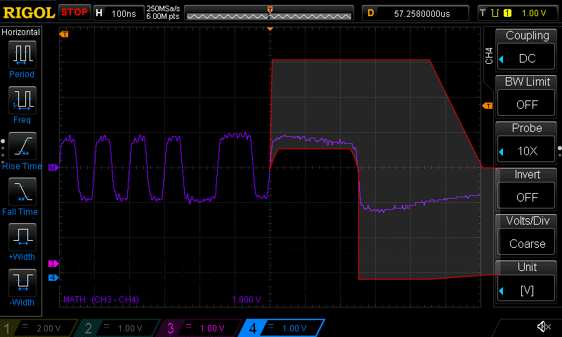
- I so far haven't been able to explain this behavior to my full complete satisfaction. I'm not even sure if I've found the right terminology to describe it. I believe it's effectively an extreme case of "baseline wander" due to the circuit being AC-coupled, where during long periods of the line being idle (i.e. a constant 0 V signal level) the signal baseline wanders higher. Once the signal has had enough transitions, its DC-balanced nature ensures that the baseline (i.e. the average signal) centers around 0 V, but that is not the case initially.
- Either way, it only takes 500 to 600 ns for the low signal level to reach the -0.585 V threshold required by the Ethernet spec, and because the preamble is so long (5600 ns) the Ethernet protocol is actually quite forgiving if the initial part of the preamble isn't received properly by a receiver. As long as a majority of the preamble is transmitted correctly, receivers should be able to successfully process the transmission.
- At the end of the transmission we see that it takes a similar 2 μs or so for the signal to settle to the idle line level of 0 V. This should be acceptable, as the IEEE 802.3 spec allows up to 45 bit times or 4.5 μs for the signal to return to 0 V.8
If we look a little more closely at the individual parts of the signal, the waveforms look quite clean, squarish and symmetrical, without significant signal noise, and with appropriate peak voltages.
An oscilloscope screenshot showing the start of the simulated outgoing packet signal, which consists of a repeating 5 MHz signal. Note the x-axis uses 200 ns time steps.
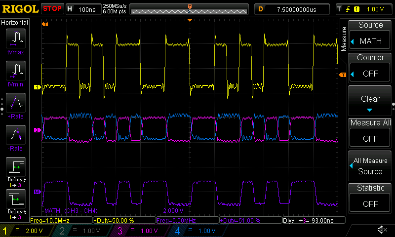
An oscilloscope screenshot showing the middle of the simulated outgoing packet signal, which consists of alternating 5 MHz and 10 MHz signals. Note the x-axis uses 100 ns time steps to show closer details of the signal waveforms.
An oscilloscope screenshot showing the end of the simulated outgoing packet signal, which consists of alternating 5 MHz and 10 MHz signals followed by a 250 ns long TP_IDL signal, followed by the line returning to its idle 0 V state. Note the x-axis uses 200 ns time steps.
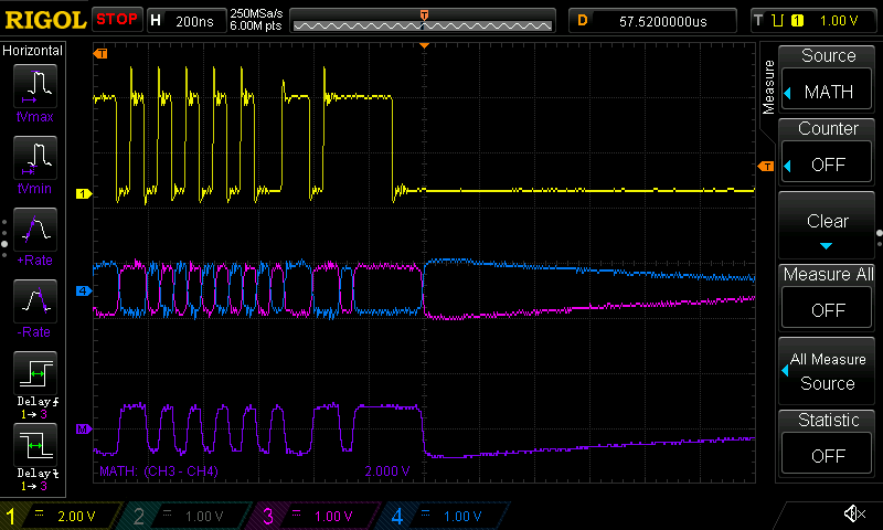
The TP_IDL waveform template
As one last validation step, we can take a closer look at the TP_IDL signal at the of the simulated data packet, as the IEEE 802.3 standard defines a waveform template for it as well, just as it did for the link test pulse.8 I've included the template below, as well as a more zoomed in view of the TP_IDL waveform with the waveform template overlaid.

The waveform template that TP_IDL pulses must fit within.
(Adapted from Figure
14–11 of the IEEE 802.3 standard document.)
An oscilloscope screenshot showing a zoomed in view of the outgoing TP_IDL waveform at the end of the simulated packet, with the waveform template overlaid. The pulse fits neatly within the template.
We can see that the generated TP_IDL waveform fits within the template with some room to spare.
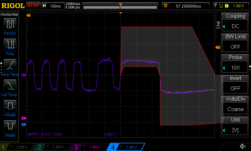
Note that this is one area where the choice of values for the AC-coupling capacitors has an important effect. As previously discussed and as shown in the next image, when using smaller 4.7 nF capacitors rather than 10 nF capacitors the latter part of the TP_IDL waveform becomes more attenuated (since the it's a lower-frequency signal that gets filtered more strongly by smaller capacitor values). As a result it gets a lot closer to the bounds of the waveform template. This is one reason why I chose to use the 10 nF capacitors: to ensure that there was sufficient leeway to account for any further signal attenuation that could occur with cables longer than the 50 ft cable I was testing with.
An oscilloscope screenshot showing the same zoomed in view of the outgoing TP_IDL waveform at the end of the simulated packet, with the waveform template overlaid, but using 4.7 nF AC-coupling capacitors instead of the 10 nF capacitors earlier. Note how the pulse still fits within the template, but only barely.
Conclusion
In the first part of this post I discussed the key components that make up all Ethernet circuits, and I shared the schematic of the circuit I chose to implement for my project.
In the second part of the post I subsequently validated that the circuit performs as it should, at least as best as we can tell at this point, by looking both at how incoming signals (link test pulses) are handled by the circuit, as well as outgoing signals (link test pulse and a simulated data packet). I also showed that by simply emitting periodic link test pulses we can already make a connected device think a link has been established.
We could still perform many more rigorous tests, as the IEEE 802.3 standard defines more waveform templates and other types of validations to ensure a transceiver is in compliance with the spec, but for my hobby project's purpose I'm more than happy to move on to actually using this circuit for real data transmissions. In my next post I'll start by showing how we can write code to transmit arbitrary data.
Footnotes
IEEE 802.3, Clause 14.4.2.2 Differential characteristic impedance.
IEEE 802.3, Clause 14.3.1.3.4 Receiver differential input impedance.
Because Manchester code ensures that there is always a signal transition for both logical 0 and 1 values, the signal will have an equal amount of high and low signal levels regardless of the data being transmitted. And of course the isolation transformers used in all Ethernet circuits introduce a form of AC-coupling, so our additional AC-coupling caps isn't really changing the situation much in that regard to begin with.
IEEE 802.3, Clause 14.3.1.2.2 Transmitter differential output impedance.
IEEE 802.3, Clause 28 Physical Layer link signaling for Auto-Negotiation on twisted pair.
My Rigol DS1054Z oscilloscope does not natively support measuring differential signals, and only supports a single MATH channel, so this is the best I can do: measuring the signals on each wire separately, tying all probes' grounds together, and using the MATH function to subtract one signal from the other.
IEEE 802.3, Figure 14–13—Transmitter waveform for link test pulse.
IEEE 802.3, Figure 14–11—Transmitter waveform for start of TP_IDL.